Electrical fingerprint sensing
Capture électrique d'empreintes digitales
Here are the fingerprint sensing techniques involving electrons interacting with the skin.
Several configurations exists:
- Passive capacitance
- Active capacitance RF field / transmission RF - capacitif actif
- Electrochemical (Prussian blue)
- Electro-optical / La lecture électro-optique
- Impedance
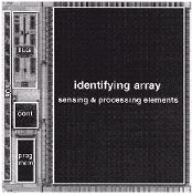
Making a fingerprint sensor based on capacitance is easy with a CMOS standard process, and many companies are proposing capacitance-based sensors, active or passive.
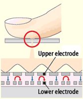
Passive Capacitance
Capacité passive
After optical sensing, the measurement of the capacitance between the skin and the pixel is the most physical effect used to acquire fingerprints. Where there is a ridge or a valley, the distance varies, as does the capacitance. Because an electrical field is measured and the distance between the skin and the pixel must be very low to provide enough sensitivity, the coating must be as thin as possible (a few microns). A significant drawback is vulnerability to strong external electrical fields, the most dangerous being ESD (Electro-Static Discharge).

Après la lecture optique, la mesure de la capacité électrique entre la peau et le pixel est l'effet physique le plus souvent mis en oeuvre: la capacité électrique varie comme l'inverse de la distance, ce qui permet de distinguer crêtes et vallées. Comme le champ électrique mesuré entre la peau et le pixel est très faible, la protection surfacique doit être très mince (quelques microns) afin d'obtenir une sensiblité correcte. Un défaut connu est la sensibilité aux forts champs électriques, comme ceux provoqués par les décharges électrostatiques ESD.
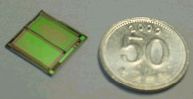
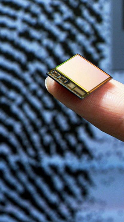
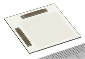
Silicon chips / puces silicium
Companies proposing (or having proposed) capacitance sensing:
Compagnies proposant (ou ayant proposé) des capteurs d'empreintes capacitifs:
- Veridicom, Fujitsu, Infineon, Sony, Upek, Hitachi, LighTuning, Melfas, Atrua, NTT, Symwave, and many other chinese companies...
Laboratories working (or having worked) on silicon capacitance sensors:
Laboratoires travaillant (ou ayant travaillés) sur les capteurs d'empreintes capacitifs:
- (1999) Seoul University A 600-dpi Capacitive Fingerprint Sensor Chip and Image-Synthesis Technique (Lee & als, Seoul National University, 1998)
- (2002) Kaist IML KAIST
- (1999) NTT NTT Microsystem Integration Laboratories
- A Single-Chip Fingerprint Sensor and Identifier (Shigematsu & als)
- (2008) Low Parasitic Capacitance
and Low-Power CMOS Capacitive Fingerprint Sensor
Department of Electrical Engineering / National Chi Nan University /Puli, Nantou, 545 Taiwan
500 dpi, 32x32 pixels.
- (2013) Design of Low Power and High Speed CMOS Fingerprint Sensor
School of Information and Telecommunication, Hanshin University, Osan, Korea
160x192 pixels.
TFT / Flat panel
Flat panel technology rather than bulk silicon has been studied by Philips Korea and some others, using capacitive sensing.
La technologie des écrans plats a été étudiée par Philips comme substitut du silicium, en utilisant un effet capacitif.
- (2003) Mitsubishi Electric Corp.
- (2004 Apr) Alps Electric develops 2 fingerprint sensors. One is transparent, electrostatic (capacitive).
Alps Electric développe 2 capteurs d'empreinte. L'un d'eux est transparent, électrostatique (capacitif). - (2017) CrossMatch unveils Nomad, a flat capacitance TFT product, 4 fingers.
RF field - Active capacitance
transmission RF - capacitif actif
Sometimes confused with capacitance sensing, the common point between RF field sensing and capacitance sensing is the "capacitance" connection of the signal.
Parfois confondu avec les capteurs capacitifs, le seul point commun entre un capteur RF et un capteur capacitif est la liaison électrique "capacitive" du signal.
A low radio frequency (RF) signal is injected into the finger, then read by the pixels on the silicon acting like antennas. The signal strenght depends on the capacitance/resistive connection, so from the distance between the skin and the pixel.
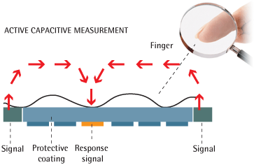
Un faible signal radiofréquence est injecté dans le doigt, puis lu par les pixels sur le silicium qui agissent comme des antennes. La puissance du signal lu dépend de la liaison capacitive/résistive, donc de la distance entre la peau et le pixel.
Many clever variations exist, particularly about the readout circuitry to increase to signal to noise ratio, especially when the coating is becoming thick (greater than the pixel pitch, so 50 microns).
Because of the required sensitivity, very often pixels are done directly on a silicon chip: it helps to have many good transistors directly where we need to read the signal. But the silicon is expensive, and it is better to have large area sensor to enhance the recognition levels. So some companies proposed to use simple copper lines (or equivalent) over a low cost substrate such as Kapton, and connect the lines to a silicon chip : silicon area is not depending on the captured fingerprint area. But at the cost of a higher noise, so a lower image quality.
Active RF sensing requires to send a signal in the skin: very often, this is done using a metal ring (e.g. Apple).
Silicon chip
Sensing pixels are directly done over a silicon chip.
Companies proposing (or having proposed) RF/AC- active capacitance sensing:
Compagnies proposant (ou ayant proposé) des capteurs d'empreintes RF:
- Authentec, Fingerprint Cards ... and many others, mainly chinese, this is becoming the principal system since Apple bought Authentec.
Labs working (or having worked) on RF capacitance sensing:
Laboratoire travaillant (ou ayant travaillé) sur les capteurs d'empreintes RF:
- Philips Korea
Low cost (non-silicon) substrate
Sensing pixels are done on an unexpensive substrate, and connected to a further silicon chip.
- Validity (now Synaptics) is offering a technology called High Frequency Co-Planar Amplitude Modulated RF Fingerprint Sensing which is using Kapton with interconnection lines for the sensing area.
- Idex was using a piece of silicon to make the connections (so not really low cost substrate...)
- Idex is now using a low cost plastic substrate, especially for smart cards.
When the frequency is zero = a constant voltage, this is the simple impedance/resistance that is used.
- (1999) Proposé par G.Olavarrieta Fritsche / SEPI-ESIME [Mexico]: A simple fingerprint sensor based on ridge conductivity.
- (2007 Mar) Imtek and Cross-Match are developping a foil sensor based on passive impedance.
Electrochemical - Prussian Blue
Bleu de Prusse
Prussian blue is known to visualize latent prints by selective electrochemical deposition:
- (2013) Visualization of latent fingerprints using Prussian blue thin films
- (2015) A Simple Chemical Method for Visualization of Sebaceous Fingerprints on Unfired Cartridge Cases by Prussian Blue Deposition
It is also possible to capture a fingerprint in one roll :
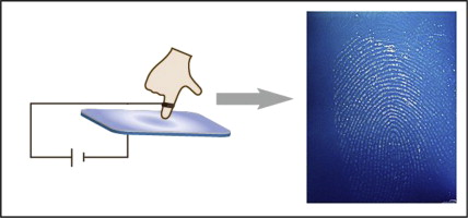
Electro-optical readers
La lecture électro-optique
Some polymers are able to emit light when properly excited with the proper voltage (generally quite a high voltage is required. This polymer is directly contacting a CMOS camera, which is necessarily the size of the finger. Generally, the finger acts as the ground, and the polymer emits light where the ridges touch. Ethentica and TesTech propose such a solution.


Certains polymères sont capables d'émettre de la lumière lorsqu'ils sont convenablement polarisé (généralement une assez haute tension est requise). Ce polymère est directement déposé sur une caméra CMOS, qui est nécessairement de la taille du doigt. En général, le doigt sert de masse, et le polymère émet de la lumière là où les crêtes touchent. Ethentica et TestTec propose ce genre de capteur.
- Heyce developped the Light emitting sensor technology around 1999-2000
- Ethentica (2001)
- TesTech, now Integrated Biometrics.
- (2017 Apr) Yonsei university did it with OLED.
- (2019 Jun) Interactive Skin Display with Epidermal Stimuli Electrode Eui Hyuk Kim & als / Yonsei university / is another version with the emissive material directly put on the skin.
Impedance (coil)
Like capacitance, it is possible to use the skin impedance characteristics, and this requires a coil to read the signal, something no so easy to manufacture with a 50 microns pitch (500 dpi).
- (2019 Nov) Usage
of the impedance effect of a spiral dual-coil for fingerprint sensor application / Shihwei Lin et al.
(The first sensor with impedance detection, one of my patents is describing this for aliveness detection a few years ago :)